Flex & Rigid-Flex Manufacturing Process
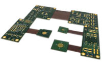
Flex and rigid-flex printed circuit boards (PCBs) offer unparalleled design flexibility, allowing for innovative solutions in various industries such as aerospace, medical devices, and consumer electronics. These PCBs are known for their ability to bend and fold, providing significant space and weight savings.
Below you will find our image gallery from the flex and rigid-flex manufacturing process. Including, material preparations, etch, drilling, plating, to final fabrication. See our blog post what it takes to manufacture flexible PCBs for more information.
Material Preparation (Pre-Clean)

Production panels chemically cleaned, prior to application of circuit forming photo resist film, to ensure proper film adhesion. Conveyorised process utilizing thin core handling equipped systems to prevent damage to ultra thin material cores.
Circuit Pattern Exposure
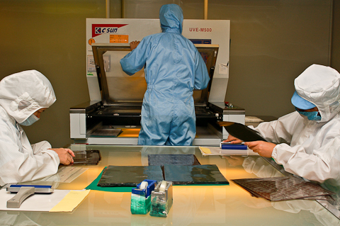
Photo resist coated panels, overlayed with circuit artwork patterns, exposed with collimated UV light to transfer circuit image(s) to production panels. Both sides exposed simultaneously if required.
Etch Process

Circuit patterns chemically etched using specialized thin core handling equipped conveyorized systems. Both sides of panels etched simultaneously if required.
Drilling Process
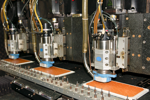
High speed, high precision, small hole capable, drilling systems create required circuit hole patterns in production panels. Laser based systems available for ultra small hole requirements.
Copper Plating Process

Fully automated electrolytic copper plating systems deposit required additional copper within plated through holes to form layer to layer electrical interconnects.
Coverlay Application

Polyimide Coverlays aligned and tacked into place on production panels prior to Coverlay lamination process.
Coverlay Lamination
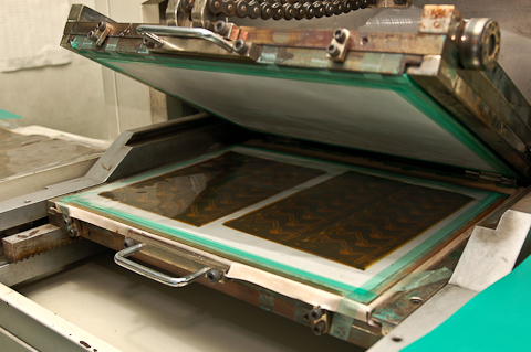
Coverlays laminated to production panels under heat, pressure and vacuum to ensure proper adhesion.
Stiffener Application

Localized additional stiffeners (if required by specific design) aligned and applied prior to additional lamination process under heat, pressure and vacuum.
Electrical Test

100% netlist driven electrical test per IPC –ET-652. Simultaneous testing of all circuits for continuity and isolation. Both grid and flying probe test systems utilized.
Final Fabrication

Individual parts die cut from production panel using high precision male / female punch and die sets. Other methods include laser cutting, mechanical routing, steel rule dies and chemically milled dies depending upon specific design requirements.
Manufacturing Process Overview
Material Preparation
Material preparation is the first critical step in the manufacturing process. This involves selecting high-quality polyimide films, copper foils, and adhesives that meet industry standards for durability and performance.
Drilling and Plating
Drilling precise holes for vias and through-holes is essential. This step ensures reliable electrical connections between different layers. After drilling, the boards undergo plating to create conductive pathways.
Imaging and Etching
In the imaging process, photoresist is applied to the substrate, and UV light is used to transfer the circuit design. Etching removes unwanted copper, leaving behind the desired circuit pattern.
Solder Mask and Surface Finish
Applying a solder mask protects the copper circuits from oxidation and helps in soldering components. The surface finish, such as ENIG (Electroless Nickel Immersion Gold), provides a reliable and solderable surface.
Technical Specifications and Standards
Our flex and rigid-flex PCBs adhere to stringent industry standards, ensuring the highest quality and reliability. These include:
- IPC-6013: This standard defines the performance and qualification requirements for flexible printed boards, ensuring that they meet rigorous quality benchmarks.
- IPC-2223: Focused on the design and implementation of flex circuits, IPC-2223 outlines best practices and technical requirements for creating reliable flexible and rigid-flex PCBs.
- MIL-P-50884: This military specification details the requirements for the manufacture of flexible and rigid-flex printed wiring boards for defense applications.
Key Specifications
- Minimum Bend Radius: The smallest radius at which the board can be bent without causing damage or functional issues.
- Maximum Layer Count: The highest number of layers our flexible PCBs can support. This is crucial for complex designs requiring multiple conductive layers.
- Temperature Range: The range of temperatures within which the flexible circuit board can operate effectively. Our products are designed to function reliably between a specific temperature range, making them suitable for harsh environments.
Additional Specifications
- Flexibility: Our flex and rigid-flex PCBs can endure repeated flexing, ensuring longevity in dynamic applications.
- Thickness: We offer various thicknesses to suit different application needs.
- Conductivity: Our materials ensure excellent electrical conductivity, meeting industry standards for performance.
Compliance and Testing
We rigorously test our flex and rigid-flex PCBs to ensure they meet all specified standards, including electrical, thermal, and mechanical stress tests. This guarantees that our products are reliable and durable in all applications, from consumer electronics to aerospace and military use.
By detailing these technical specifications and standards, we provide a comprehensive understanding of the capabilities and quality of our flex and rigid-flex PCBs.
Unsure of the Flex PCB Manufacturing Process?
Discover the intricacies of flex and rigid-flex pcb manufacturing to help you navigate your next project with confidence. Contact Epec for a custom solution.
Request a Quote Request Design Support Request More Information